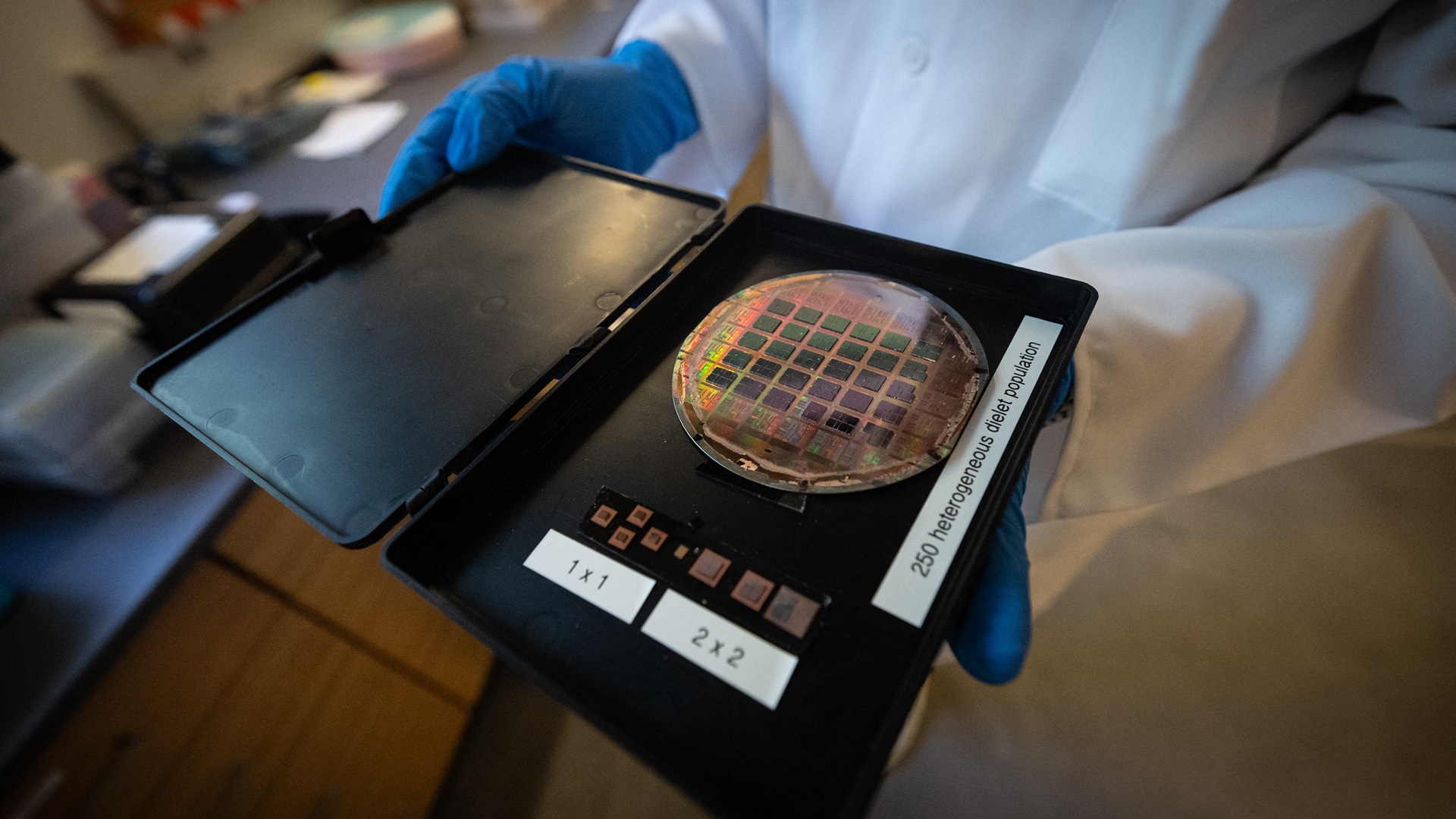
The U.S. Department of Commerce plans to invest up to $140 million in semiconductor equipment maker Multibeam to develop next-generation chip packaging technologies aimed at keeping American chipmakers competitive in the AI era. The proposed funding, announced through a Letter of Intent under the CHIPS Research and Development Office, will support research into fine-pitch advanced packaging process flows that allow multiple chips to be integrated more closely. The goal is to help U.S. semiconductor companies build faster and more energy-efficient computing systems as demand for artificial intelligence and high-performance computing continues to grow. Rather than relying solely on shrinking transistors to improve chip performance, the industry is increasingly turning to advanced packaging, where several specialized chips, or chiplets, are combined into a single package. This approach enables manufacturers to improve computing performance while overcoming the physical limits of traditional chip scaling. Multibeam said the project will build on advances in semiconductor manufacturing equipment to develop dense chip-to-chip interconnections and wafer-scale integrated systems that could eventually incorporate hundreds of chiplets. The company added that the technology is intended to shorten development cycles for custom computing systems while improving power efficiency. Beyond transistor scaling For decades, improvements in wafer fabrication equipment drove Moore’s Law by enabling chipmakers to pack more transistors onto silicon. As those gains become harder to achieve, advanced packaging has emerged as a key technology for continuing improvements in computing performance. Multibeam has assembled a consortium of U.S.-based industry partners with expertise in semiconductor manufacturing, testing equipment and chip architectures. Together, they aim to develop new manufacturing process flows capable of supporting increasingly complex heterogeneous systems, including those integrating silicon photonics and other specialized components. “With today’s compute supply chain investments, the Trump Administration is accelerating America’s innovation engine,” said Secretary of Commerce Howard Lutnick. “These strategic investments will enhance our country’s domestic capabilities, create high-paying jobs and keep America at the forefront of the semiconductor industry.” The Department of Commerce said the proposed investment is intended to strengthen domestic capabilities in advanced semiconductor packaging while supporting the development of next-generation computing platforms. Strengthening domestic chipmaking Bill Frauenhofer, Executive Director for Semiconductor Innovation and Investment at the Department of Commerce, said the project could help remove long-standing bottlenecks in advanced packaging. “The CHIPS R&D incentives will support a breakthrough in compute and communication networks moving past traditional advanced packaging bottlenecks,” Frauenhofer said. “Accelerating R&D for domestic advanced packaging integration of photonics capabilities and novel system architectures provides American industry the extreme bandwidth and energy efficiency to scale complex AI workloads.” Multibeam said its MBX multi-column electron-beam lithography platform allows rapid design changes during chip development while supporting increasingly complex heterogeneous device architectures. According to the company, the platform can reduce chip-to-chip power consumption by more than ten times compared with conventional approaches.“Working in concert with the U.S. Department of Commerce and our hardware and software partners, we are excited to provide a new innovation and manufacturing capability to U.S. innovators that will enable rapid development of purpose-built multi-chip systems, accelerating the path from idea to production,” said Ken MacWilliams, president of Multibeam.Recommended ArticlesGet the latest in engineering, tech, space & science - delivered daily to your inbox.With over a decade-long career in journalism, Neetika Walter has worked with The Economic Times, ANI, and Hindustan Times, covering politics, business, technology, and the clean energy sector. Passionate about contemporary culture, books, poetry, and storytelling, she brings depth and insight to her writing. When she isn’t chasing stories, she’s likely lost in a book or enjoying the company of her dogs.
US launches $140M initiative for advanced chip packaging and wafer-scale systems
Full Article
Original Source
Read the full article at Interestingengineering →KhanList aggregates and links to publicly available news content. We do not host full articles from third-party sources. Always verify important information with original sources.