
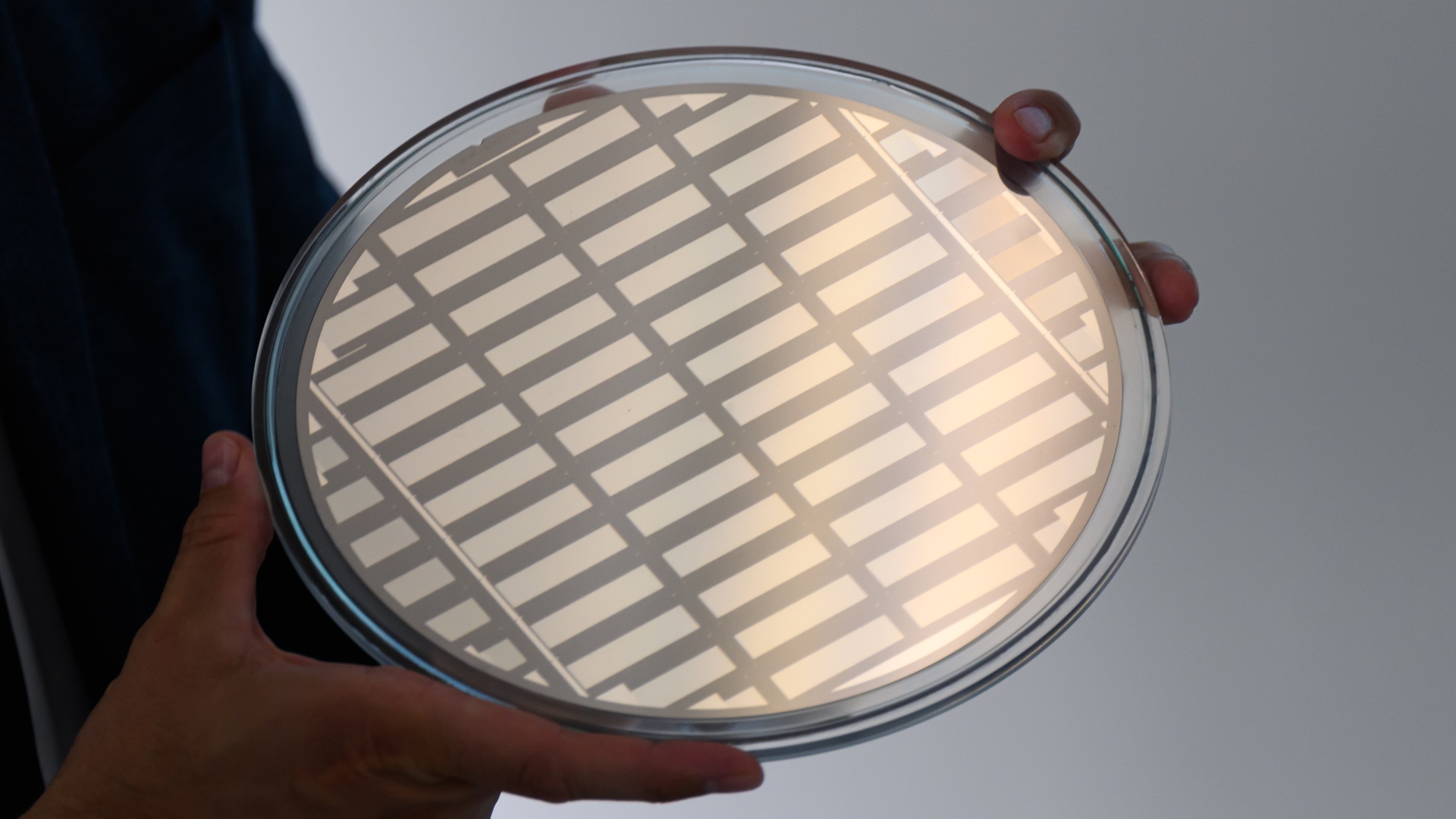
Researchers have developed a tiny semiconductor device that can change the frequency, or color, of light far more efficiently than conventional designs, potentially shrinking components used in telecommunications and quantum technologies. The device combines specially engineered semiconductor layers with a nanoscale metasurface. Together, they concentrate and control light inside the material, producing an effective nonlinear optical response up to three orders of magnitude higher than that of an unpatterned wafer. The work tackles a longstanding problem in photonics. Frequency conversion allows one color of light to be converted into another, but conventional systems often depend on materials such as lithium niobate or gallium arsenide and can be difficult to make compact and scalable. The researchers instead designed the material and the optical structure at the same time. This allowed them to control the electronic properties of the semiconductor, the electromagnetic fields and the geometry of the device to improve light conversion at specific wavelengths. Engineering light at nanoscale The team built the semiconductor from gallium arsenide and aluminum gallium arsenide, arranging the materials into ultra-thin layers known as multi-quantum wells. These layers were engineered to create electronic energy levels that strengthen interactions between light and matter. The researchers then added an array of tiny nanopillars to the surface. The resulting metasurface shapes and concentrates the electromagnetic field inside the semiconductor, increasing the intensity of light interacting with the material. The nanopillars also control the symmetry of the electromagnetic fields. This is important because some optical interactions can otherwise cancel each other out. Together, the engineered quantum wells and metasurface produced a nonlinear response three orders of magnitude higher than the unpatterned wafer. The researchers demonstrated the effect at near-infrared wavelengths, a range that is important for fiber-optic communications. “This work combines, in a creative way, quantum engineering of an underlying material and enhancing its nonlinearity, together with optimized metasurface design,” Capasso said. “The overall nonlinear response is greatly enhanced and made usable for free-space optics.” Smaller components, broader uses The approach could make frequency-conversion devices much smaller while retaining efficient light conversion. Such components could generate wavelengths that are difficult to produce directly with lasers. The technology could also be useful for photonic quantum systems. The researchers point to potential applications including sources of entangled photon pairs for quantum communication and computation. Another advantage is that the platform uses compound semiconductor materials and planar nanofabrication, making it compatible with existing semiconductor manufacturing processes. That could make the approach easier to integrate into compact photonic devices. Collaborators at the University of Texas at Austin developed the multi-quantum-well material, while researchers at Harvard designed the metasurface and the electromagnetic fields within the structure. “This initial demonstration opens the door for so much more to be done at the intersection of nanophotonics and materials science,” said Pernille Undrum Fathi, a Ph.D. student in Capasso’s lab and first author of the paper. The research was a collaboration between Harvard John A. Paulson School of Engineering and Applied Sciences, the University of Texas at Austin, and the University of California, Irvine. The study was published in Nature Nanotechnology. Get the latest in engineering, tech, space & science - delivered daily to your inbox.With over a decade-long career in journalism, Neetika Walter has worked with The Economic Times, ANI, and Hindustan Times, covering politics, business, technology, and the clean energy sector. Passionate about contemporary culture, books, poetry, and storytelling, she brings depth and insight to her writing. When she isn’t chasing stories, she’s likely lost in a book or enjoying the company of her dogs.
New metasurface boosts light conversion in tiny semiconductor device by 1,000x
Full Article
Original Source
Read the full article at Interestingengineering →KhanList aggregates and links to publicly available news content. We do not host full articles from third-party sources. Always verify important information with original sources.